


Nanofabrication: Creating Structures at the Nanoscale
Nanofabrication is the process of creating structures and devices at the nanoscale, typically ranging from 1 to 100 nanometers. It involves manipulating and controlling matter at the atomic and molecular level to fabricate materials and devices with unique properties and functionalities. Nanofabrication techniques have revolutionized various fields, including electronics, medicine, energy, and materials science.
Top-down and Bottom-up Approaches
Nanofabrication can be achieved through two main approaches: top-down and bottom-up. The top-down approach involves starting with a larger structure and gradually reducing its size to the nanoscale. This method typically involves techniques such as lithography, etching, and deposition. On the other hand, the bottom-up approach involves building structures atom by atom or molecule by molecule. This approach includes techniques such as self-assembly, molecular beam epitaxy, and chemical vapor deposition.
Lithography: Patterning at the Nanoscale
Lithography is one of the most widely used techniques in nanofabrication. It involves selectively removing or adding material to create patterns on a substrate. In photolithography, a photosensitive material called a photoresist is exposed to light through a mask, creating a pattern that is transferred to the substrate. Electron beam lithography uses a focused beam of electrons to directly write patterns on the substrate. These techniques enable the creation of intricate patterns with high precision and resolution.
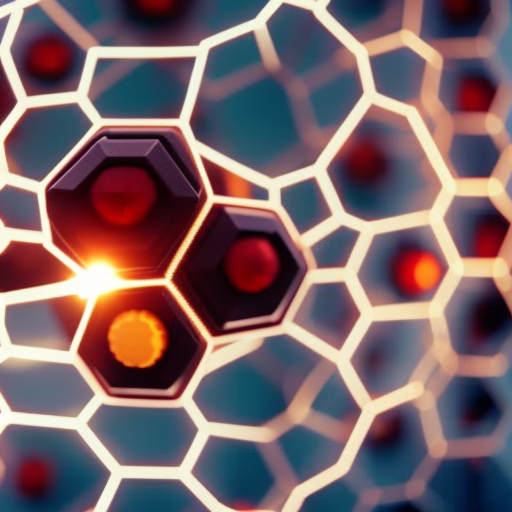
Self-Assembly: Nature’s Blueprint
Self-assembly is a bottom-up approach inspired by nature’s ability to organize matter at the nanoscale. It involves designing and synthesizing molecules or nanoparticles that can spontaneously arrange themselves into desired structures. This technique offers a cost-effective and scalable method for creating complex nanostructures. Self-assembled structures have applications in areas such as drug delivery, nanoelectronics, and nanophotonics.
Molecular Beam Epitaxy: Growing Crystals Atom by Atom
Molecular beam epitaxy (MBE) is a technique used to grow thin films of crystalline materials with atomic precision. It involves evaporating atoms or molecules from a heated source and depositing them onto a substrate in a vacuum chamber. MBE enables the growth of high-quality materials with well-defined crystal structures, making it essential for the development of semiconductor devices, quantum dots, and superconductors.
Applications of Nanofabrication
Nanofabrication has revolutionized various fields and enabled the development of advanced technologies. In electronics, nanofabrication has led to the miniaturization of transistors, allowing for faster and more powerful computer chips. Nanofabrication techniques have also been used to create sensors with high sensitivity and selectivity, enabling advancements in healthcare, environmental monitoring, and food safety.
In medicine, nanofabrication has opened up new possibilities for targeted drug delivery, tissue engineering, and diagnostics. Nanoparticles can be functionalized to specifically target cancer cells, delivering drugs directly to the tumor while minimizing side effects. Nanofabrication techniques have also been used to create artificial tissues and organs, offering potential solutions for organ transplantation.
In the energy sector, nanofabrication has played a crucial role in the development of more efficient solar cells, batteries, and fuel cells. Nanomaterials with unique properties, such as high surface area and enhanced catalytic activity, have been used to improve energy conversion and storage devices.
Nanofabrication has also had a significant impact on materials science. By manipulating the structure and composition of materials at the nanoscale, researchers have been able to create materials with enhanced mechanical, electrical, and optical properties. These materials have applications in areas such as aerospace, automotive, and construction industries.
In conclusion, nanofabrication is a powerful tool for creating structures and devices at the nanoscale. It offers unique opportunities for developing advanced technologies in various fields. Whether through top-down techniques like lithography or bottom-up approaches like self-assembly, nanofabrication has the potential to shape the future of science and technology.